The Drum · Weekly AI news, freeSubscribe →

Share
As planar scaling runs out of road, the semiconductor industry's top research conference showcased exotic fixes, from atomically thin 2D-material transistors to chips stacked and bonded in three dimensions to keep performance gains coming.
Moore's Law isn't dead, but it's definitely not getting any easier. That was the subtext running through this year's IEEE International Electron Devices Meeting (IEDM), the conference where the chip industry airs its most forward-looking research a solid 5 to 10 years before any of it shows up in a product you can buy.
If you've been following semiconductor news, you know the story by now: shrinking transistors the old-fashioned way, just making the same planar structures smaller, stopped scaling cleanly over a decade ago. The industry's response has been architectural reinvention rather than brute-force shrinkage. FinFETs gave way to gate-all-around nanosheet transistors. Now the next frontier is going vertical, literally stacking devices and even entire chips on top of each other, while also experimenting with entirely new channel materials that can be engineered at the atomic scale.
Two threads dominated this year's presentations: 2D semiconductor materials that could eventually replace silicon in the transistor channel, and 3D integration techniques that stack multiple layers of logic, memory, or entire dies to pack more computing into the same footprint. Neither is a drop-in replacement for what's running in fabs today. Both are serious bets on where performance gains have to come from once you can't just make things smaller.
Here's the core problem: transistor density has kept climbing, but interconnect, the wiring that actually moves signals and power around a chip, hasn't kept pace. At advanced nodes, the wires themselves have become a bigger bottleneck than the transistors. Shrinking a wire makes it thinner, which increases resistance, which slows signals down and burns more power. You can't just scale your way out of that one.
3D stacking sidesteps the problem by changing the geometry of the whole system. Instead of spreading transistors across a single flat die and routing signals ever-longer distances laterally, you stack multiple dies or device layers vertically and connect them with much shorter vertical interconnects. Shorter wires mean lower resistance, less latency, and less power wasted just moving data from one part of a chip to another.
This isn't theoretical. The industry has already shipped 3D stacking in production parts:
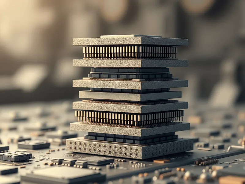
What IEDM presenters were pushing further is finer-grained 3D integration, stacking not just whole chips but individual transistor layers and even stacking logic directly on memory with much tighter bonding pitches than today's commercial packaging allows. The tighter the bond pitch, the shorter the vertical interconnect, and the closer you get to behaving like one continuous piece of silicon instead of two chips glued together.
That tighter integration is hard. Bonding two wafers together with micrometer-scale alignment, managing the heat generated by stacking power-hungry logic directly on top of more logic or memory, and keeping yield high across multiple bonded layers are all open engineering problems. If one layer in a stack has a defect, do you scrap the whole stack? Thermal management gets particularly nasty: stack enough compute vertically and you create a hotspot problem that's much harder to cool than a single flat die with more surface area exposed to a heatsink.
On the materials side, 2D semiconductors are being explored as a way to keep transistor channels thin without losing electrical performance. Silicon channels get electrically leaky as they get thinner, current leaks where it shouldn't, wasting power and degrading performance. Materials like transition metal dichalcogenides (TMDs) can, in principle, stay atomically thin while maintaining better electrostatic control over the channel than silicon can at the same thickness. That property matters a lot if you're trying to stack transistor layers vertically, since thinner layers with good control make vertical integration more practical.
None of this is remotely close to replacing silicon CMOS in production. 2D-material transistors at IEDM are still largely academic demonstrations: single devices or small test arrays, not anything resembling a yielding, mass-producible process. The gap between a working lab device and a billion-transistor chip that ships reliably for years is enormous, and that gap is exactly what IEDM papers exist to chip away at, one incremental result at a time.
The throughline across this year's IEDM is that the industry has largely accepted that 2D scaling, just making transistors smaller on a flat plane, has hit diminishing returns. Future performance gains are increasingly going to come from geometry (stacking in 3D) and materials innovation (new channels beyond silicon) rather than straightforward shrinkage.
For practitioners, the practical near-term relevance is in the 3D integration work. HBM and chiplet-based 3D stacking are already shipping, and the tighter-pitch, finer-grained stacking techniques discussed at IEDM represent the next few generations of that same trajectory, not a clean break from it. The 2D-materials research is the longer bet, genuinely interesting, scientifically meaningful, but likely a decade or more from showing up in anything you'd actually design around.
If you're tracking where chip performance gains are heading next, watch the packaging and integration side at least as closely as the transistor side. The wires, and how you stack and connect them, have become just as important as the devices they connect.
Tags
Original Sources
3D Chip Stacking
↗ https://spectrum.ieee.org/iedm/3d-chip-stacking
About the author
Kai built ML infrastructure at a Bay Area startup before developing an obsession with transformer architectures and inference optimisation that eventually pulled him out of product work entirely. A stint at a compute research lab sharpened his instinct for what actually matters in a model release versus what is marketing. He writes from the inside — from the perspective of someone who has debugged the systems he is describing at three in the morning. He is allergic to hype and instinctively drawn to the unglamorous plumbing questions that everyone else skips over.
More from The Engineer →This Week's Edition
6 November 2026
28 articles
Related Articles
Related Articles
More Stories
© 2026 Cedar & Bloom. All rights reserved.