The Drum · Weekly AI news, freeSubscribe →

Share
GPUs are packing more silicon than ever, but hitting a trillion transistors won't come from shrinking gates alone. Packaging, chiplets, and 3D stacking are doing the heavy lifting now.
GPU transistor counts have basically exploded over the last decade, and the industry's next milestone, a trillion-transistor chip, is now openly discussed as a "when" rather than an "if." Nvidia's Blackwell GPU already packs 208 billion transistors. Get to a trillion and you're looking at roughly a 5x jump from where we are today. The interesting part isn't the number itself. It's how we're going to get there, because the old playbook of just shrinking transistors on a single monolithic die is running out of road.
For decades, Moore's Law delivered more transistors per chip mostly through pure geometric scaling: make the transistor smaller, cram more of them into the same area. That approach is hitting real physical limits. Silicon's crystal lattice parameter is about 0.543 nanometers, and as one commenter on the original IEEE Spectrum piece pointed out, there's a hard floor on how far you can shrink a gate before you run into the physics of the material itself. So the industry has been quietly shifting strategy: instead of one giant die, you build multiple smaller dies, called chiplets, and stitch them together into something that behaves like a single giant chip.
That's exactly what's happening with GPUs aimed at AI workloads. Nvidia's Blackwell architecture uses two dies connected by a high-bandwidth interface, effectively acting as one logical GPU. This is a packaging problem as much as a fabrication problem now. Advanced packaging techniques like CoWoS (Chip-on-Wafer-on-Substrate) from TSMC let you place multiple compute dies and memory stacks side by side or vertically, wired together with much shorter, denser interconnects than anything you could achieve going off-package. Think of it as shrinking the "PCB" down to a package-level structure instead of a full circuit board.
Here's the practical reason this matters to anyone building or scaling AI systems: raw compute has been outpacing memory for a while now, and that imbalance shapes every design decision.
This is part of why the "trillion transistor GPU" framing isn't just about cramming more logic onto silicon. It's about integration: how you connect compute dies, memory stacks, and interconnect fabric so the whole package behaves efficiently. Chiplet-based designs let you mix and match process nodes too. You can build your logic dies on a bleeding-edge node while keeping I/O or analog components on a cheaper, more mature process, which helps with yield and cost.
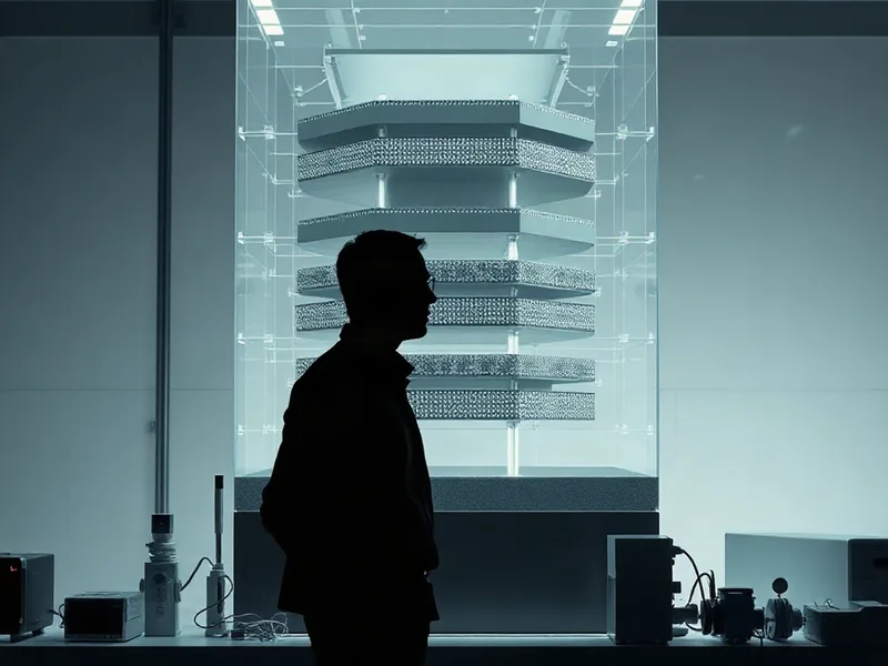
That yield question is a real tension though. Chiplet architectures add packaging complexity and testing overhead that monolithic dies don't have. More interconnects between dies means more places for something to go wrong, and stacking dies vertically (3D integration) introduces thermal and power delivery challenges that engineers are still working through. It's not a free lunch, it's a trade of one set of engineering headaches for another.
There's also a fair amount of skepticism worth acknowledging here. Whether the industry needs this scale of compute at all is genuinely contested. The value proposition of ever-larger LLMs hasn't fully proven out yet, and some researchers are betting on entirely different paradigms, like neuromorphic computing, which promises efficiency gains of six orders of magnitude or more by mimicking biological neural structures rather than brute-forcing more transistors. If that bet pays off, a chunk of this trillion-transistor push could end up looking like overbuilt infrastructure for a problem that got solved differently.
Cost is the other side of that coin. Advanced packaging and chiplet integration aren't cheap, and yield losses on complex multi-die assemblies can eat into the economic case for this approach. But there's also a straightforward economic argument in the other direction: as compute costs continue to fall on a per-FLOP basis, even with rising design complexity, it opens the door to applications and research that were previously too expensive to justify. Historically that's exactly what's driven adoption curves in computing, cheaper compute enables experimentation that wasn't viable before.
The trillion-transistor milestone will almost certainly get hit within the next several years, but the path there says more about the industry's priorities than the number itself. Watch for:
The real story isn't that chips are getting bigger. It's that "bigger" now means something architecturally different than it did a decade ago, and the winners in this next phase will be the companies that master integration, not just transistor shrinkage.
Tags
Original Sources
Toward a Trillion Transistors
↗ https://spectrum.ieee.org/trillion-transistor-gpu/toward-a-trillion-transistors?itm_source=summaries&itm_medium=ieee-spectrum&itm_campaign=summary-toward-a-trillion-transistors&itm_content=summary-reduce
About the author
Kai built ML infrastructure at a Bay Area startup before developing an obsession with transformer architectures and inference optimisation that eventually pulled him out of product work entirely. A stint at a compute research lab sharpened his instinct for what actually matters in a model release versus what is marketing. He writes from the inside — from the perspective of someone who has debugged the systems he is describing at three in the morning. He is allergic to hype and instinctively drawn to the unglamorous plumbing questions that everyone else skips over.
More from The Engineer →This Week's Edition
6 September 2026
24 articles
Related Articles

Tether Evo's New Research Tackles BCI's Cross-Subject Problem Across Speech, Vision, and Music
Models & Research · 6 min

xAI Launches Grok Bot, an Autonomous Agent That Logs Into Your Tools and Does the Work
Products & Applications · 5 min

German Bishops Back Child-Friendly AI Standards, Citing Papal Call on Human Dignity
Policy & Regulation · 5 min
Related Articles
Tether Evo's New Research Tackles BCI's Cross-Subject Problem Across Speech, Vision, and Music
Models & Research · 6 min
xAI Launches Grok Bot, an Autonomous Agent That Logs Into Your Tools and Does the Work
Products & Applications · 5 min
German Bishops Back Child-Friendly AI Standards, Citing Papal Call on Human Dignity
Policy & Regulation · 5 min
More Stories
© 2026 Cedar & Bloom. All rights reserved.