The Drum · Weekly AI news, freeSubscribe →

Share
As transistor scaling hits physical and economic walls, chipmakers are betting on vertical integration instead. Here's why stacking logic, memory, and I/O in the z-axis is becoming the default path forward for AI hardware.
For decades, the industry's answer to "how do we make chips faster" was basically one word: smaller. Shrink the transistor, pack more of them per square millimeter, collect your performance win. That playbook is running out of road. Classic 2D scaling is bumping against atomic-scale limits, and the cost per transistor at the bleeding edge has stopped reliably falling the way it used to. So engineers are doing something that sounds almost obvious in hindsight: instead of only going wider, they're going up.
3D chip stacking, building vertically by bonding multiple dies or wafers on top of each other, has been a research topic for years. What's changed is urgency. AI workloads need more compute and more memory bandwidth packed into tighter power and area budgets than Moore's Law alone can deliver anymore. Stacking gives architects a new axis to work with, and the semiconductor industry is now treating it less like a moonshot and more like a roadmap item.
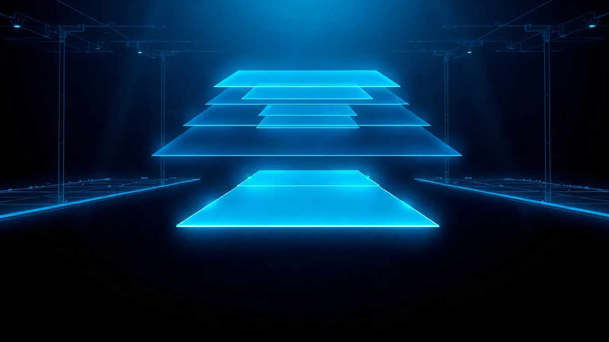
The appeal is straightforward once you think about it in terms of interconnect distance. In a traditional 2D layout, a logic die and a memory die sit side by side on a package, and data has to travel laterally across the substrate, through package traces, before it even reaches the other chip. That trip costs both latency and energy. Stack the dies instead, and you shrink that distance from millimeters to microns. Vertical interconnects, often through-silicon vias (TSVs) or hybrid copper bonding, can move data over paths thousands of times shorter than their planar equivalents.
That distance reduction isn't just a nice-to-have for benchmarks. It directly attacks two of the biggest bottlenecks in modern AI silicon: memory bandwidth and power delivery.
Large language models and other AI workloads are frequently memory-bound, not compute-bound. The GPU or accelerator sits idle waiting for data to move in and out of memory, and a huge chunk of the energy budget for a chip goes into shuttling bits across the die-to-die interface rather than doing math on them. High-Bandwidth Memory (HBM) stacks already exploit this principle by stacking DRAM dies vertically with TSVs to widen the memory interface dramatically compared to planar DDR layouts. 3D stacking extends that same logic to logic-on-logic and logic-on-memory integration more broadly.
A few technical threads are converging to make this practical at scale:

Foundries and IDMs are already shipping or sampling stacked designs commercially, not just in research papers. HBM is the most visible example and has become essential infrastructure for AI accelerators from the major GPU vendors, since a single accelerator's performance is often gated by how much memory bandwidth you can feed it. Beyond memory, logic-on-logic stacking, where you take a chip that would traditionally be one monolithic die and split it into two or more stacked tiers, is also moving from research demos toward production, with chipmakers presenting process and reliability data at conferences like IEDM (the IEEE International Electron Devices Meeting) that specifically focuses on this kind of advanced packaging and 3D integration work.
The tradeoffs are real, though, and worth being honest about. Yield math gets trickier: if you're bonding together, say, four dies and each one has some probability of being defective, the net yield of the stacked assembly compounds across all of them, unless you can test and bin good dies before bonding, which adds its own cost and complexity. Thermal density goes up, since you're packing more active silicon into the same footprint, which means more heat to extract from a smaller volume. And testing an already-stacked assembly for defects is harder than testing a single flat die, because you lose some of the probe access you'd normally have.
None of that is a dealbreaker. It's an engineering tax that the industry is actively working to reduce, the same way it worked through yield and testing challenges for earlier packaging innovations like flip-chip and 2.5D interposer designs. The direction of travel is clear: vertical integration is no longer a niche technique reserved for memory stacks. It's becoming a core tool in the broader toolbox for building AI infrastructure, alongside advanced process nodes and chiplet-based architectures.
3D stacking shortens the physical distance data has to travel between logic and memory from millimeters down to microns, directly addressing the memory-bandwidth and power bottlenecks that plague AI accelerators. Hybrid bonding and TSVs are the key enabling interconnect technologies, while thermal management and backside power delivery are the parallel innovations needed to make dense vertical stacks actually work in production. Yield and testing remain real engineering challenges, but the industry's trajectory, visible in both commercial HBM deployments and research presented at venues like IEDM, points toward vertical integration becoming a standard tool for AI hardware design rather than a specialized exception.
Tags
Original Sources
3D Chip Stacking
↗ https://spectrum.ieee.org/iedm/3d-chip-stacking
About the author
Kai built ML infrastructure at a Bay Area startup before developing an obsession with transformer architectures and inference optimisation that eventually pulled him out of product work entirely. A stint at a compute research lab sharpened his instinct for what actually matters in a model release versus what is marketing. He writes from the inside — from the perspective of someone who has debugged the systems he is describing at three in the morning. He is allergic to hype and instinctively drawn to the unglamorous plumbing questions that everyone else skips over.
More from The Engineer →This Week's Edition
18 October 2026
24 articles
Related Articles

Microsoft Unveils Maia 300, Its Next AI Inference Chip, With Multi-Gigawatt Rollout Planned for 2027
Tools & Engineering · 5 min

Why AI Pilots Stall: Enterprises Are Missing a Decision Layer, Not a Better Model
Tools & Engineering · 5 min
xAI Launches Grok Bot, an Autonomous Agent That Logs Into Your Tools and Does the Work
Products & Applications · 5 min
Related Articles
Microsoft Unveils Maia 300, Its Next AI Inference Chip, With Multi-Gigawatt Rollout Planned for 2027
Tools & Engineering · 5 min
Why AI Pilots Stall: Enterprises Are Missing a Decision Layer, Not a Better Model
Tools & Engineering · 5 min
xAI Launches Grok Bot, an Autonomous Agent That Logs Into Your Tools and Does the Work
Products & Applications · 5 min
More Stories
© 2026 Cedar & Bloom. All rights reserved.