The Drum · Weekly AI news, freeSubscribe →
Share
Moore's Law scaling sideways is running out of road, so AMD, Intel, and Graphcore are stacking silicon vertically instead. Here's what that means for latency, power, and how you should think about future hardware.
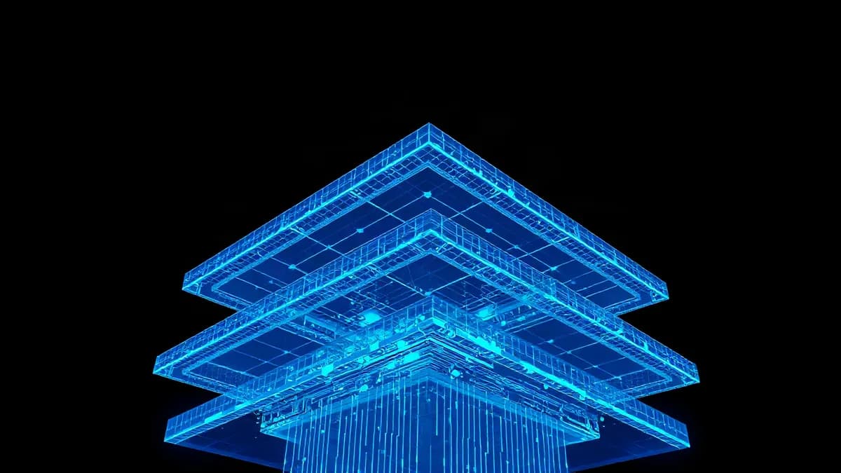
For decades, the industry played the same game: shrink the transistor, cram more of them onto a flat piece of silicon, ship a faster chip. That game is getting brutally expensive to keep winning. Each new process node costs more to develop, yields less improvement, and takes longer to reach volume production. So a handful of major chipmakers are trying something different: instead of making chips bigger and flatter, they're stacking them.
3D chip stacking isn't a brand-new idea, but it's finally moving from lab curiosity to shipping product. AMD, Intel, and Graphcore are each taking it in slightly different directions, and the implications for anyone doing performance-sensitive engineering, from ML training to HPC workloads, are significant.
The core problem 3D stacking solves is one every systems engineer already knows intuitively: the further data has to travel, the more time and energy it costs you. On a traditional 2D chip, cores, cache, and I/O are laid out side by side, and signals have to physically traverse that distance. Stack the dies vertically instead, and you shorten those interconnects dramatically. Shorter wires mean lower latency and lower power draw for the same operation, which is exactly the kind of free lunch engineers have been chasing since Dennard scaling started running out of steam.
AMD's approach centers on its 3D V-Cache technology, which it's already shipping in production. Rather than redesigning the entire chip, AMD stacks additional SRAM cache directly on top of the compute die using through-silicon vias (TSVs), tiny vertical electrical connections drilled through the silicon layers. The benefit is straightforward: more cache sitting physically closer to the cores that need it, which matters enormously for workloads that are cache-sensitive, think large in-memory databases or certain gaming workloads with big working sets.
Intel's play is more structural. Its Foveros packaging technology lets the company mix and match chiplets, small, specialized dies, made on different process nodes and stack them together into one package. This is a big deal for cost control: instead of manufacturing an entire monolithic chip on the newest, most expensive process node, Intel can put only the parts that actually benefit from cutting-edge lithography (like the compute logic) on the advanced node, while cheaper components (I/O, memory controllers) sit on older, less expensive processes in the same stack. That's a meaningfully different economic model than "build everything on the bleeding edge and eat the cost."
Graphcore, the UK-based AI chip startup, is pushing 3D integration specifically for its Intelligence Processing Units (IPUs), chips purpose-built for machine learning workloads. Graphcore's bet is that stacking lets them pack in more processing elements and memory bandwidth than a flat design could support, which is the exact bottleneck that limits a lot of AI training hardware today. Memory bandwidth, not raw compute, is often the real ceiling on how fast you can train large models, so any architecture that meaningfully improves the compute-to-memory pathway is worth watching closely.

There's real technical substance behind the "40 percent improvement" figures that get thrown around in coverage of this space, though the actual gains are workload-dependent, and it's worth being skeptical of any single benchmark number presented without context. One commenter on the original IEEE Spectrum piece pointed to work from Alibaba and IC League showing gains that reportedly exceed the commonly cited 40 percent figure, which is a useful reminder that this field is moving fast across multiple players, not just the usual Western chipmakers. China's semiconductor ecosystem is investing heavily in 3D integration as a way to leapfrog process-node limitations they can't easily overcome through lithography access alone.
There's also a manufacturing wrinkle worth flagging for anyone who's spent time around fab terminology: "pitch," in the context of these interconnects, refers to the distance from one edge of a trace (a conductive line) to the corresponding edge of the next trace, essentially the minimum width plus the minimum spacing between traces. Getting pitch small enough to support dense TSV arrays without cross-talk or yield problems is one of the genuine engineering headaches behind all this stacking. It's not just "glue two chips together", the interconnect density and thermal management at these scales are nontrivial problems that packaging engineers are still working through.
Thermal management, in fact, might be the underappreciated challenge here. When you stack compute dies on top of each other, you're concentrating heat generation in a smaller physical footprint, and getting that heat out efficiently becomes a much harder problem than it is on a flat, spread-out die. Expect a lot of the next few years of 3D stacking innovation to be as much about thermal engineering and power delivery as it is about the logic design itself.
3D stacking isn't a single technology, it's a family of approaches, and the differences matter. AMD is using it to solve a cache-latency problem in existing architectures. Intel is using it to decouple process-node choice from chip design, which has real cost implications. Graphcore is betting on it to break the memory-bandwidth bottleneck that constrains AI accelerators specifically.
For practitioners, the takeaway is less "which company wins" and more "this is now a durable direction for the industry." If you're evaluating hardware for latency-sensitive or memory-bound workloads in the next few years, vertical integration is going to show up in the spec sheet, and understanding what's actually stacked, cache, logic, or memory, will matter more than the marketing number attached to it.
Tags
Original Sources
3 Ways 3D Chip Tech is Upending Computing
↗ https://spectrum.ieee.org/amd-3d-stacking-intel-graphcore/particle-4
About the author
Kai built ML infrastructure at a Bay Area startup before developing an obsession with transformer architectures and inference optimisation that eventually pulled him out of product work entirely. A stint at a compute research lab sharpened his instinct for what actually matters in a model release versus what is marketing. He writes from the inside — from the perspective of someone who has debugged the systems he is describing at three in the morning. He is allergic to hype and instinctively drawn to the unglamorous plumbing questions that everyone else skips over.
More from The Engineer →This Week's Edition
6 September 2026
24 articles
Related Articles

Microsoft Unveils Maia 300, Its Next AI Inference Chip, With Multi-Gigawatt Rollout Planned for 2027
Tools & Engineering · 5 min

3D Chip Stacking Moves From Lab Curiosity to Production Necessity
Tools & Engineering · 6 min

Why AI Pilots Stall: Enterprises Are Missing a Decision Layer, Not a Better Model
Tools & Engineering · 5 min
Related Articles
Microsoft Unveils Maia 300, Its Next AI Inference Chip, With Multi-Gigawatt Rollout Planned for 2027
Tools & Engineering · 5 min
3D Chip Stacking Moves From Lab Curiosity to Production Necessity
Tools & Engineering · 6 min
Why AI Pilots Stall: Enterprises Are Missing a Decision Layer, Not a Better Model
Tools & Engineering · 5 min
More Stories
© 2026 Cedar & Bloom. All rights reserved.