The Drum · Weekly AI news, freeSubscribe →
Share
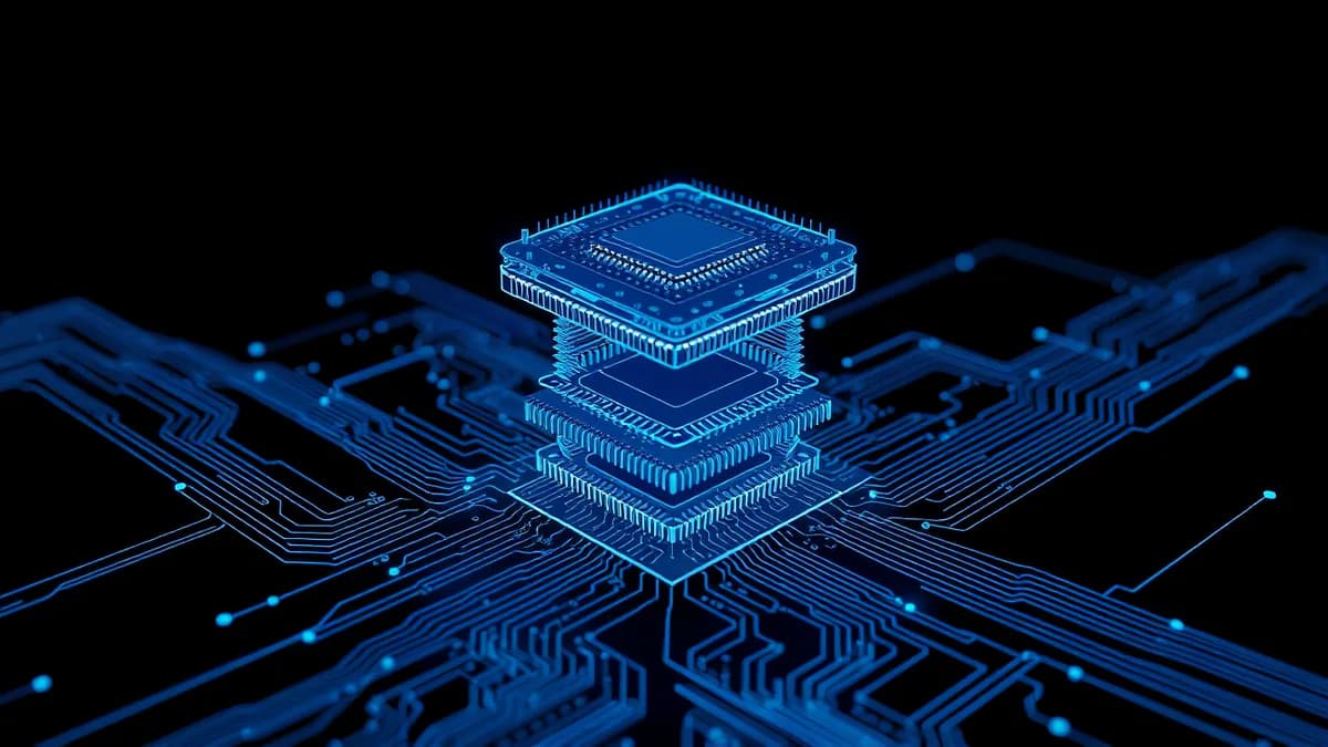
At IEDM this year, researchers made the case that the industry's future isn't thinner transistors but taller chips, stacking logic, memory, and new 2D materials to keep performance climbing once planar scaling hits its physical limits.
For decades, the semiconductor industry's playbook was simple: shrink the transistor, cram more of them onto a die, repeat. That formula is running out of road. At this year's IEEE International Electron Devices Meeting (IEDM), the conversation has shifted decisively toward a different axis of scaling entirely, up.
The core problem is physics, not ambition. Transistor gates are approaching dimensions where quantum effects, leakage current, and heat dissipation start to dominate the engineering tradeoffs. You can keep shrinking features for a few more process nodes, but the returns are diminishing fast and the cost per transistor is no longer reliably dropping the way it did in the golden years of Moore's Law.
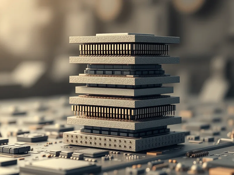
So the industry is doing what it's done before when one dimension gets tapped out: adding another one. 3D chip stacking, bonding multiple layers of silicon vertically instead of spreading everything out flat, lets designers pack more compute and memory into the same footprint without needing a smaller transistor. It's a structural workaround for a problem that lithography alone can't solve anymore.
This isn't a brand-new idea. High Bandwidth Memory (HBM) stacks have been shipping in GPUs and AI accelerators for years, and chiplet designs from AMD and Intel already glue separate dies together on a single package. What's different now is the scope of ambition on display at IEDM: researchers are pushing toward finer-grained 3D integration, stacking logic directly on logic, not just memory on top of a processor, and doing it with interconnect density that starts to blur the line between "two chips on a package" and "one chip."
Stacking dies vertically does more than save space. It fundamentally changes the interconnect math that governs chip performance.
In a traditional 2D layout, signals traveling between, say, a CPU core and its cache have to go through long horizontal wires. Those wires add latency and burn power, and the problem gets worse as chips get bigger. Stack the cache directly on top of the core instead, and that same signal travels a fraction of the distance, straight up through a via instead of sideways across a die.
That's the appeal in a nutshell: shorter wires mean lower latency, lower power draw per bit moved, and more bandwidth between layers than you could ever route on a flat surface. For memory-bound workloads, AI training and inference chief among them, that vertical bandwidth is often the actual bottleneck, not raw compute.
A few technical threads are converging to make this practical at scale:
None of this is free. Bonding yield matters a lot more when you're stacking five known-good dies versus betting on one monolithic chip; a single bad layer can tank an entire stack's economics. Testing also gets harder: you need to verify each die before bonding, since you can't easily access buried layers once they're sealed into a stack. These are solvable problems, but they require investment in process control and test infrastructure that's different from what fabs have optimized for over the last 20 years.
It's worth putting this in context with where the industry already is. HBM3 stacks eight or twelve DRAM dies and delivers bandwidth well beyond what any single planar memory chip could achieve, which is exactly why it's become standard in AI accelerators from Nvidia and AMD. The IEDM work extends that same logic further down the stack, toward logic-on-logic integration rather than just memory-on-logic.
The throughline from IEDM this year is that 2D scaling and 3D integration aren't competing strategies, they're complementary ones. Shrinking transistors still matters, and new channel materials like 2D semiconductors could extend that runway further. But vertical stacking is no longer a niche trick reserved for memory; it's becoming a first-class design axis for logic too.
For engineers working anywhere near chip design or systems architecture, the practical implication is this: the performance gains of the next few years are increasingly going to come from packaging and integration decisions, not just process node announcements. Expect EDA tooling, thermal design, and bonding yield to matter as much to a chip's final performance as the transistor spec sheet. The transistor isn't going away as the unit of progress, but it's sharing the stage with how those transistors get stacked, connected, and cooled.
Tags
Original Sources
3D Chip Stacking
↗ https://spectrum.ieee.org/iedm/3d-chip-stacking
About the author
Kai built ML infrastructure at a Bay Area startup before developing an obsession with transformer architectures and inference optimisation that eventually pulled him out of product work entirely. A stint at a compute research lab sharpened his instinct for what actually matters in a model release versus what is marketing. He writes from the inside — from the perspective of someone who has debugged the systems he is describing at three in the morning. He is allergic to hype and instinctively drawn to the unglamorous plumbing questions that everyone else skips over.
More from The Engineer →This Week's Edition
2 October 2026
28 articles
Related Articles
Payerset Bets on AI Research Assistant to Make Price Transparency Data Usable
Products & Applications · 6 min

China's Biotech Sector Stakes Its Claim on the Global Stage
Finance & Markets · 5 min

Blue Shield of California Signals Commercial Expansion of Medicare's ACCESS Chronic Care Model
Health & Science · 5 min
Related Articles
Payerset Bets on AI Research Assistant to Make Price Transparency Data Usable
Products & Applications · 6 min
China's Biotech Sector Stakes Its Claim on the Global Stage
Finance & Markets · 5 min
Blue Shield of California Signals Commercial Expansion of Medicare's ACCESS Chronic Care Model
Health & Science · 5 min
More Stories
© 2026 Cedar & Bloom. All rights reserved.